Showing posts with label Solid State Electronics. Show all posts

Wednesday, June 9, 2010

Forward and reverse bias in pn junctions

We now consider a p-n diode with an applied bias voltage, Va. A forward bias corresponds to applying a positive voltage to the anode (the p-type region) relative to the cathode (the n-type region). A reverse bias corresponds to a negative voltage applied to the cathode. Both bias modes are illustrated with Figure below. The applied voltage is proportional to the difference between the Fermi energy in the n-type and p-type quasi-neutral regions. As a negative voltage is applied, the potential across the semiconductor increases and so does the depletion layer width. As a positive voltage is applied, the potential across the semiconductor decreases and with it the depletion layer width. The total potential across the semiconductor equals the built-in potential minus the applied voltage,

The built-in potential

The built-in potential in a semiconductor equals the potential across the depletion region in thermal equilibrium. Since thermal equilibrium implies that the Fermi energy is constant throughout the p-n diode, the built-in potential equals the difference between the Fermi energies, EFn and EFp, divided by the electronic charge. It also equals the sum of the bulk potentials of each region, fn and fp, since the bulk potential quantifies the distance between the Fermi energy and the intrinsic energy. This yields the following expression for the built-in potential.
Example 2 An abrupt silicon p-n junction consists of a p-type region containing 2 x 10^16 cm-3 acceptors and an n-type region containing also 10^16 cm-3 acceptors in addition to 10^17 cm-3 donors. 1. Calculate the thermal equilibrium density of electrons and holes in the p-type region as well as both densities in the n-type region. 2. Calculate the built-in potential of the p-n junction 3. Calculate the built-in potential of the p-n junction at 400 K..
Solution where the instrinsic carrier density at 400 K was obtained from example1 1. The thermal equilibrium densities are: In the p-type region: p = Na = 2 x 10^16 cm-3 n = ni^2/p = 10^20/2 x 10^16 = 5 x 103 cm-3 In the n-type region n = Nd - Na = 9 x 10^16 cm-3 p = ni2/n = 10^20/(1 x 10^16) = 1.11 x 10^3 cm-3 2 The built-in potential is obtained from: 3.Similarly, the built-in potential at 400 K equals:

Thermal equilibrium for pn junctions

To reach thermal equilibrium, electrons/holes close to the metallurgical junction diffuse across the junction into the p-type/n-type region where hardly any electrons/holes are present. This process leaves the ionized donors (acceptors) behind, creating a region around the junction, which is depleted of mobile carriers. We call this region the depletion region, extending from x = -xp to x = xn. The charge due to the ionized donors and acceptors causes an electric field, which in turn causes a drift of carriers in the opposite direction. The diffusion of carriers continues until the drift current balances the diffusion current, thereby reaching thermal equilibrium as indicated by a constant Fermi energy. This situation is shown in Figure below While in thermal equilibrium no external voltage is applied between the n-type and p-type material, there is an internal potential, fi, which is caused by the workfunction difference between the n-type and p-type semiconductors. This potential equals the built-in potential, which will be further discussed in the next section

Flatband diagram of pn Junctions

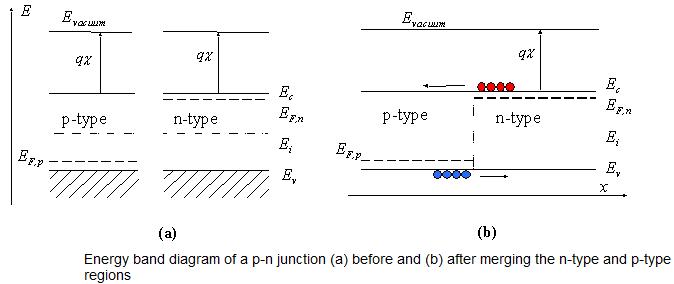
The principle of operation will be explained using a gedanken experiment, an experiment, which is in principle possible but not necessarily executable in practice. We imagine that one can bring both semiconductor regions together, aligning both the conduction and valence band energies of each region. This yields the so-called flatband diagram shown in Figure below Note that this does not automatically align the Fermi energies, EF,n and EF,p. Also, note that this flatband diagram is not an equilibrium diagram since both electrons and holes can lower their energy by crossing the junction. A motion of electrons and holes is therefore expected before thermal equilibrium is obtained. The diagram shown in Figure above (b) is called a flatband diagram. This name refers to the horizontal band edges. It also implies that there is no field and no net charge in the semiconductor.

Structure and principle of operation of pn junction

A p-n junction consists of two semiconductor regions with opposite doping type as shown in Figure below. The region on the left is p-type with an acceptor density Na, while the region on the right is n-type with a donor density Nd. The dopants are assumed to be shallow, so that the electron (hole) density in the n-type (p-type) region is approximately equal to the donor (acceptor) density. We will assume, unless stated otherwise, that the doped regions are uniformly doped and that the transition between the two regions is abrupt. We will refer to this structure as an abrupt p-n junction. Frequently we will deal with p-n junctions in which one side is distinctly higher-doped than the other. We will find that in such a case only the low-doped region needs to be considered, since it primarily determines the device characteristics. We will refer to such a structure as a one-sided abrupt p-n junction. The junction is biased with a voltage Va as shown in Figure above. We will call the junction forward-biased if a positive voltage is applied to the p-doped region and reversed-biased if a negative voltage is applied to the p-doped region. The contact to the p-type region is also called the anode, while the contact to the n-type region is called the cathode, in reference to the anions or positive carriers and cations or negative carriers in each of these regions.

 
Powered by Blogger