Showing posts with label Semi-conductors Materials. Show all posts

Wednesday, June 9, 2010

Forward and reverse bias in pn junctions

We now consider a p-n diode with an applied bias voltage, Va. A forward bias corresponds to applying a positive voltage to the anode (the p-type region) relative to the cathode (the n-type region). A reverse bias corresponds to a negative voltage applied to the cathode. Both bias modes are illustrated with Figure below. The applied voltage is proportional to the difference between the Fermi energy in the n-type and p-type quasi-neutral regions. As a negative voltage is applied, the potential across the semiconductor increases and so does the depletion layer width. As a positive voltage is applied, the potential across the semiconductor decreases and with it the depletion layer width. The total potential across the semiconductor equals the built-in potential minus the applied voltage,

The built-in potential

The built-in potential in a semiconductor equals the potential across the depletion region in thermal equilibrium. Since thermal equilibrium implies that the Fermi energy is constant throughout the p-n diode, the built-in potential equals the difference between the Fermi energies, EFn and EFp, divided by the electronic charge. It also equals the sum of the bulk potentials of each region, fn and fp, since the bulk potential quantifies the distance between the Fermi energy and the intrinsic energy. This yields the following expression for the built-in potential.
Example 2 An abrupt silicon p-n junction consists of a p-type region containing 2 x 10^16 cm-3 acceptors and an n-type region containing also 10^16 cm-3 acceptors in addition to 10^17 cm-3 donors. 1. Calculate the thermal equilibrium density of electrons and holes in the p-type region as well as both densities in the n-type region. 2. Calculate the built-in potential of the p-n junction 3. Calculate the built-in potential of the p-n junction at 400 K..
Solution where the instrinsic carrier density at 400 K was obtained from example1 1. The thermal equilibrium densities are: In the p-type region: p = Na = 2 x 10^16 cm-3 n = ni^2/p = 10^20/2 x 10^16 = 5 x 103 cm-3 In the n-type region n = Nd - Na = 9 x 10^16 cm-3 p = ni2/n = 10^20/(1 x 10^16) = 1.11 x 10^3 cm-3 2 The built-in potential is obtained from: 3.Similarly, the built-in potential at 400 K equals:

Thermal equilibrium for pn junctions

To reach thermal equilibrium, electrons/holes close to the metallurgical junction diffuse across the junction into the p-type/n-type region where hardly any electrons/holes are present. This process leaves the ionized donors (acceptors) behind, creating a region around the junction, which is depleted of mobile carriers. We call this region the depletion region, extending from x = -xp to x = xn. The charge due to the ionized donors and acceptors causes an electric field, which in turn causes a drift of carriers in the opposite direction. The diffusion of carriers continues until the drift current balances the diffusion current, thereby reaching thermal equilibrium as indicated by a constant Fermi energy. This situation is shown in Figure below While in thermal equilibrium no external voltage is applied between the n-type and p-type material, there is an internal potential, fi, which is caused by the workfunction difference between the n-type and p-type semiconductors. This potential equals the built-in potential, which will be further discussed in the next section

Sunday, June 6, 2010

Temperature dependence of the energy bandgap

The energy bandgap of semiconductors tends to decrease as the temperature is increased. This behavior can be understood if one considers that the interatomic spacing increases when the amplitude of the atomic vibrations increases due to the increased thermal energy. This effect is quantified by the linear expansion coefficient of a material. An increased interatomic spacing decreases the average potential seen by the electrons in the material, which in turn reduces the size of the energy bandgap. A direct modulation of the interatomic distance - such as by applying compressive (tensile) stress - also causes an increase (decrease) of the bandgap. The temperature dependence of the energy bandgap, Eg, has been experimentally determined yielding the following expression for Eg as a function of the temperature, T: where Eg(0), a and b are the fitting parameters. These fitting parameters are listed for germanium, silicon and gallium arsenide in Table below A plot of the resulting bandgap versus temperature is shown in Figure below for germanium, silicon and gallium arsenide.
Example 1 Calculate the energy bandgap of germanium, silicon and gallium arsenide at 300, 400, 500 and 600 K.
Solution The bandgap of silicon at 300 K equals: Similarly one finds the energy bandgap for germanium and gallium arsenide, as well as at different temperatures, yielding:

Saturday, June 5, 2010

The Kronig-Penney model

The Kronig-Penney model demonstrates that a simple one-dimensional periodic potential yields energy bands as well as energy band gaps. While it is an oversimplification of the three-dimensional potential and bandstructure in an actual semiconductor crystal, it is an instructive tool to demonstrate how the band structure can be calculated for a periodic potential, and how allowed and forbidden energies are obtained when solving the corresponding Schrödinger equation. The Kronig-Penney consists of an infinite series of rectangular barriers with potential height, V0, and width, b, separated by a distance, a-b, resulting in a periodic potential with period, a. The analysis requires the use of Bloch functions, traveling wave solutions multiplied with a periodic function, which has the same periodicity as the potential Solutions for k and E are obtained when the following equation is satisfied:

This equation can only be solved numerically. Solutions are only obtained if the function, F, is between -1 and 1 since it has to equal cos(ka). The energy, E, is plotted as function of ka/p and the function F in Figure

The corresponding band structure is shown below (black curve) as well as the energy for a free electron (gray curve). Three different forms are presented, namely the E(k) digram, the E(k diagram combined with the reduced-zone diagram as well as the reduced-zone diagram only. From Figure above.a we observe the following: The E(k) relation resembles a parabola except that only specific ranges of energies are valid solutions to Schrödinger's equation and therefore are allowed, while others are not. The range of energies for which there is no solution is referred to as an energy band gap. The transitions between allowed and forbidden energies occur at non-zero integer multiples of ka/p. These correspond to local minima and maxima of the E(k) relation. The reduced-zone diagram shown in Figure above.c contains the first three bands and energy bandgaps. For instance the second energy bandgap occurs between 1.5 and 2 eV, between the band maximum of the second band and the band minimum of the third band.

Periodic potentials

The analysis of periodic potentials is required to find the energy levels in a semiconductor. This requires the use of periodic wave functions, called Bloch functions which are beyond the scope of this text. The result of this analysis is that the energy levels are grouped in bands, separated by energy band gaps. The behavior of electrons at the bottom of such a band is similar to that of a free electron. However, the electrons are affected by the presence of the periodic potential. The combined effect of the periodic potential is included by adjusting the value of the electron mass. This mass will be referred to as the effective mass. The effect of a periodic arrangement on the electron energy levels is illustrated by Figure below Shown are the energy levels of electrons in a carbon crystal with the atoms arranged in a diamond lattice. These energy levels are plotted as a function of the lattice constant, a. Isolated carbon atoms contain six electrons, which occupy the 1s, 2s and 2p orbital in pairs. The energy of an electron occupying the 2s and 2p orbital is indicated on the figure. The energy of the 1s orbital is not shown. As the lattice constant is reduced, there is an overlap of the electron wavefunctions occupying adjacent atoms. This leads to a splitting of the energy levels consistent with the Pauli exclusion principle. The splitting results in an energy band containing 2N states in the 2s band and 6N states in the 2p band, where N is the number of atoms in the crystal. A further reduction of the lattice constant causes the 2s and 2p energy bands to merge and split again into two bands containing 4N states each. At zero Kelvin, the lower band is completely filled with electrons and labeled as the valence band. The upper band is empty and labeled as the conduction band.

Free electron model

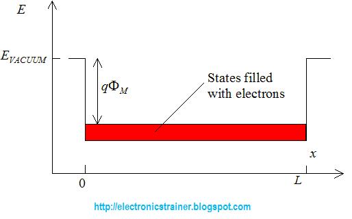
The free electron model of metals has been used to explain the photo-electric effect . This model assumes that electrons are free to move within the metal but are confined to the metal by potential barriers as illustrated by Figure below. The minimum energy needed to extract an electron from the metal equals qFM, where FM is the workfunction. This model is frequently used when analyzing metals. However, this model does not work well for semiconductors since the effect of the periodic potential due to the atoms in the crystal has been ignored.

a)The free electron model of a metal

 
Powered by Blogger